
News
ServicesNext-generation
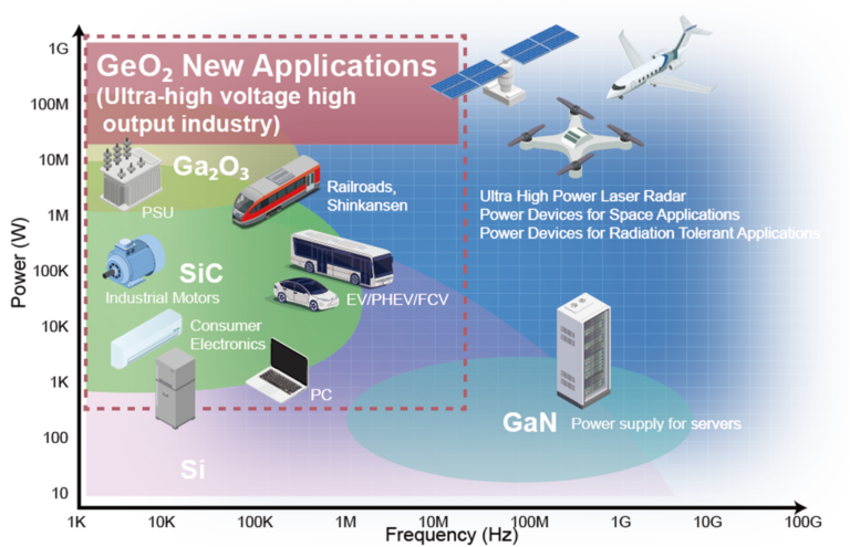
power semiconductor: GeO₂
GeO2 has five crystalline polymorphisms: a rutile structure, an α-quartz structure, a CaCl2 type, an α-PbO2 type, and a pyrite type. Among them, the rutile structure r-GeO2 has a huge band gap of 4.6 eV, with both n-type and p-type conduction being theoretically predicted.
As such it is expected to be applicable to next generation high-performance Normally-off MOSFETs, among others. On the other hand, the trigonal α-quartz structure GeO2 has a very large band gap of 6.2eV and exhibits piezoelectricity.
As such, it is expected to be applicable as an HEMT element for next-generation Schottky barrier diodes and high-capacity, high-speed 7G communications, which will come after 6G.
Low loss / Compact size
Semiconductor materials with large forbidden bands (band gaps) tend to have large dielectric breakdown field strengths. On the other hand, as a rule of thumb, there is a trade-off relationship between the size of the band gap and the density of major carriers. The larger the band gap, the more the material behaves as an insulator, and the less it exhibits electrical properties as a semiconductor. Searching for materials that have a high balance of these contradictory properties forms an important guideline in the research of new power semiconductor materials. Our company focuses on germanium dioxide (GeO₂), which is currently under development, and aim to implement it in society.
High voltage resistance
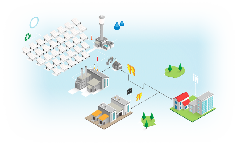
As GeO₂ has a large band gap and is expected to be produced at low cost in both bulk and thin membranes, it is expected to create a market for high voltage resistance and high output, which is difficult to achieve with existing materials. For example, it is expected to be used in the creation of ultra-high output power supply and motors, small inverters, power devices for outer space, radiation-resistant power devices, etc.
Advantages of GeO2 as a power semiconductor
P-type and n-type dopabilties applicable to normally-off GeO₂ MOSFETs.
Inexpensive bulk crystals and epitaxial layers
UWBG semiconductor with high potential as a power semiconductor
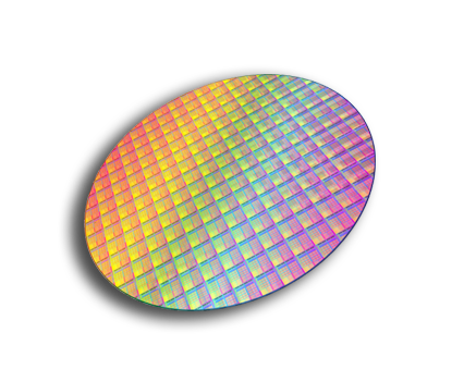
GeO2 Semiconductor Products
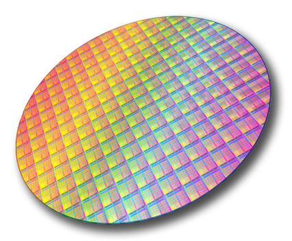
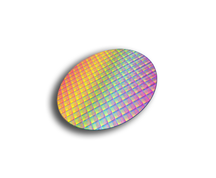
6inch substrate
(Under development)
4inch Epi wafer/substrate
(Under development)
2inch Epi wafer/substrate
(Under development)
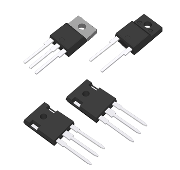
Power devices
(Under development)
Crystal growth system/ Thin film fabrication services
- PhantomSVD(Phantom Spatial Vapor Deposition) equipment: Crystal growth equipment based on new principles evolved from the mist CVD method
- Phantom surface processing equipment for roughening, etc.: safe, inexpensive, highly efficient, and high quality
- Development and improvement services for novel functional membranes (new metal oxide membranes, new metal membranes, new organic membranes, etc.)